FlatSat Meeting
What is a ‘FlatSat’ Meeting?
At some stage during the development of a new satellite, it becomes necessary to bring all the sub assemblies together and make sure that they work together (both mechanically and electrically) as expected and desired.
In most satellites these assemblies are printed circuit boards (PCBs), and these are stacked for maximum packing density.
Having them stacked in this way is not ideal during development, as it becomes difficult or impossible to attach measuring probes (e.g. oscilloscopes, voltmeters, etc.) as there just is not room between the boards.
Howard and Graham unpack the EM at the start of the weekend (video)
Hence the term flat sat, where the PCBs are laid flat on a bench, and interconnected with extension leads. Of course, this isn’t truly representative of how they will operate in the finished satellite (e.g. we may not detect some electromagnetic radiation (EMC) problems, but if they don’t work in flat sat mode, they probably won’t work in stacked mode.
We coined the name FUNsquare for this meeting, on the basis that the flatsat would be two-dimensional, rather than three-dimensional.
Where and When
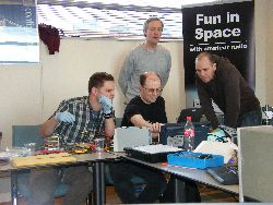
The meeting took place over the weekend of 10/11 April 2010. Most of the developers attended both days, and stayed in a nearby hotel overnight. The meeting was kindly hosted by Graham in the main conference room of his company office, near Tottenham Court Road in London.
“What – surely you need a large lab, with lots of test equipment for such an activity?” you might say. Well, yes and no. Our satellite is only small (10cm x 10 cm x 10 cm) and weighs less than 1.2 kg, so the component parts are small, light and easy to transport. All the test equipment, soldering station, power supplies, etc. were bought by the developers. Modern test equipment is quite small and light, although we had one elderly and heavy HP spectrum analyser as well! The coffee was generously supplied by Graham.
Who Are these developers
OK, lets introduce the team – see this page.
Did you really have ALL the components to test
No, the only parts that were missing were the RF board and PA board. These are still being produced. What we did have in their place was a simulator which took the signals (telemetry – tlm) from the CCT board, applied the modulation as it would be done in the final version of the RF board, and produced an output on 10.7 MHz (which it would do in the ‘real thing’). The part we didn’t have was the up-converter to 145 MHz, or the Power Amplifier (PA) to boost the signal to the expect output level. We had to use an existing external up-converter and PA to do this.
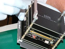
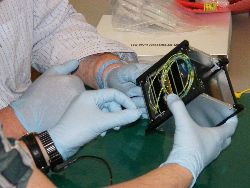
What we DID have, which was extremely useful was a real satellite structure and EPS (Electronic Power System) which AMSAT has purchased from ISIS. This item is EXACTLY the same as will eventually fly, so we were able to check many things against it, e.g. we proved that the CCT board mechanical design, including the PC104 connector location, size etc. was compatible. We did this by physically fitting the CCT board into the structure (called an Engineering Model (EM), because it probably won’t ever actually fly – but see below).
We were also able to check that the EPS was capable of powering the CCT board, and yes it did, perfectly. As a matter of fact the power consumption of the CTT board was less than 11 mA at 3.3V. Given its functionality, this is a very low figure.
Why did we wear rubber gloves to handle the EM Structure?
It’s just possible that the EM might fly some day. For example, we might possibly have a FUNcube -2 one day! Wearing rubber gloves ensures that the chemicals from our hands, don’t come into contact with the surfaces of the EM. If they did, they might, over time, react with the metal of the structure producing things like oxides, which in turn might affect the electrical properties of the structure.
OK, so what did we set out to achieve?
Here’s what we AIMED to do:
1. Power up CCT board, and confirm correct operation
2. Power up I2C simulator/EPS board and confirm correct operation
3. Connect I2C Sim/EPS board to CCT board, and check data flow.
4. Power Up 10.7 MHz simulator and check operation OK
5. Connect 10.7 MHz sim to CCT board and check output on 10.7 MHz (audio only)
6. Deleted
7. Connect 4 x thermistors to CCT board, and check that when cooled/warmed CCT board can measure the difference.
7a If using EPS, check that CCT board is measuring things like change in charging rate, etc
For Sunday
8. Connect 10.7 –> 145 MHz converter.
9. Check audio OP on 2m Rx
10. Connect SSB Rx to LapTop running demod software.
11. Check that tlm readings are displayed on LapTop
12. Alter inputs to CCT board, eg thermistor temp, EPS voltages, etc, check that tlm displayed on laptop respond.
13. Deleted
14. Set up and test USB rx, check signals rxed and demodulated OK
Diagramatically

Testing the connection of the EPS to the CT Board. L to R, Wouter, Phil, Michael (standing), DuncanDiagramatically
EPS -> CCT I2C Master -> CCT FEC encoder -> CCT PWM Modulator -> 10.7MHz Tx -> 145MHz Tx -> 145MHz SSB Rx -> PC decoder -> PC FEC Decoder -> PC Real time TLM display
Did we do all this?
In a word NO. Did we do almost all of it? YES, we did! Which bits didn’t we do? The only bits we didn’t do were
– connect the thermistors to the CCT board. We decided to do this with potentiometers as we had no good way of cooling/warming the thermistors.
– in the limited time available we didn’t successfully get the tlm from the EPS into the CCT board. We suspect that there is a minor CCT board software tweak which is needed.
BUT all the rest we achieved absolutely perfectly, so importantly we tested all the interfaces, including the very sophisticated, error correcting, modulation system. Moment of success (video) – Close up of screen with audio of signal from satellite
Were we pleased with the result?
Yes, extremely, the outcome of this meeting is that we have gained in confidence very significantly, and we are now looking forward to the next similar meeting where we hope to be able to stack all of the PCBs, as they will be physically and electrically just the same as those that will fly.
Further information:
There are more photos (G3VZV and G3WGM) here and more videos here


