Structure
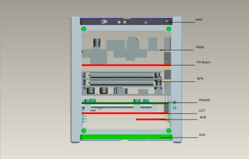
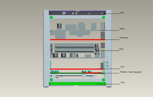
30th October 2010 – Here are some more pictures showing two possible general arrangements of the satellite. Until further analysis of thermal and other issues has been completed the final stack sequence will not be confirmed.
The picture above shows the arrangement of the PCB within the “stack”. The AntS (at the top) is not a PCB, but a bolt on narrow box housing the antenna deployer mechanism. The item labelled IGIS at the bottom is also not a PCB, but a box onto which the ABF/RBF (Apply Before Flight/Remove Before Flight) plugs can be mounted. These plugs allow things such as battery charging whilst the satellite is waiting for launch, and also does things like inhibit antenna deployment before the launch. The B0B is a small PCB allowing the IGIS to connect to the PC104 bus. The PCB labelled PMASS, houses the permanent magnet and dampers for stabilisation about the Z axis. The picture below shows the same arrangement, but without the BoB which might not be required.
FUNcube Structure – First flight hardware.
We have recently (February 2010) received the picture below from our contractor. They are of the two sides of the main CubeSat structure.
They are differently coloured to facilitate the Materials Science Experiment – see this page for more info on this.
You can see on the picture two small holes in the sides of the frames, these are where the separation switches are mounted, and is also where we plan to mount 2 of the 4 thermistors to measure the temperature of the structure.


